
Predicting Nanometer Defects in Semiconductor Manufacturing
We use real-world manufacturing data to train proprietary AI models to eliminate microscopic defects, saving chip fabs equipment capital, labour cost and time.






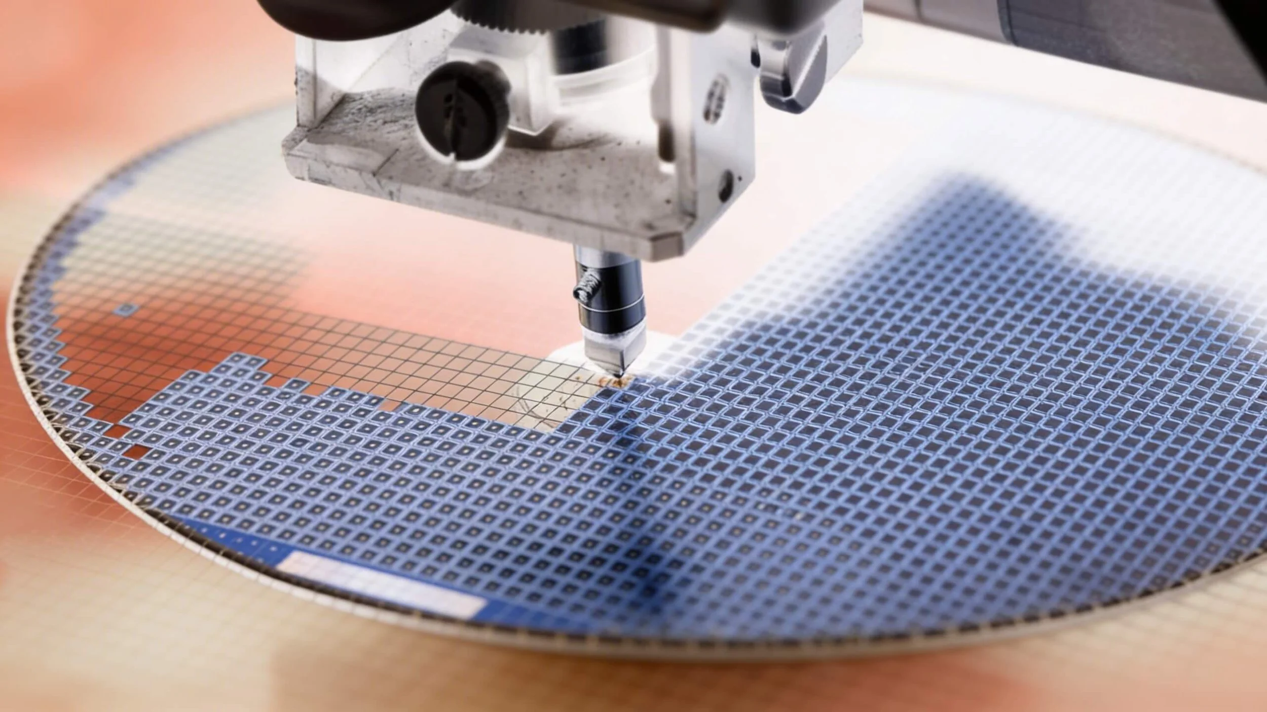
The Opportunity
Semiconductor fabs spend billions and months optimising fabrication through trial and error.
A Complexity Barrier
Fabricating modern chips involves over 2,000 steps with sub-5nm precision. Optimising a fabrication process involves extensive trial-and-error iterations, wasted time and high operational costs.
The Yield Problem
Device yield in chip manufacturing can be lower than 50%.
The Financial Toll
This inefficiency results in tens of billions in lost revenue every year.
The Limitation
The accuracy of traditional modelling is constrained by our limited understanding of the fabrication process at the atomic scale.
Our Solution
Data Driven Modelling
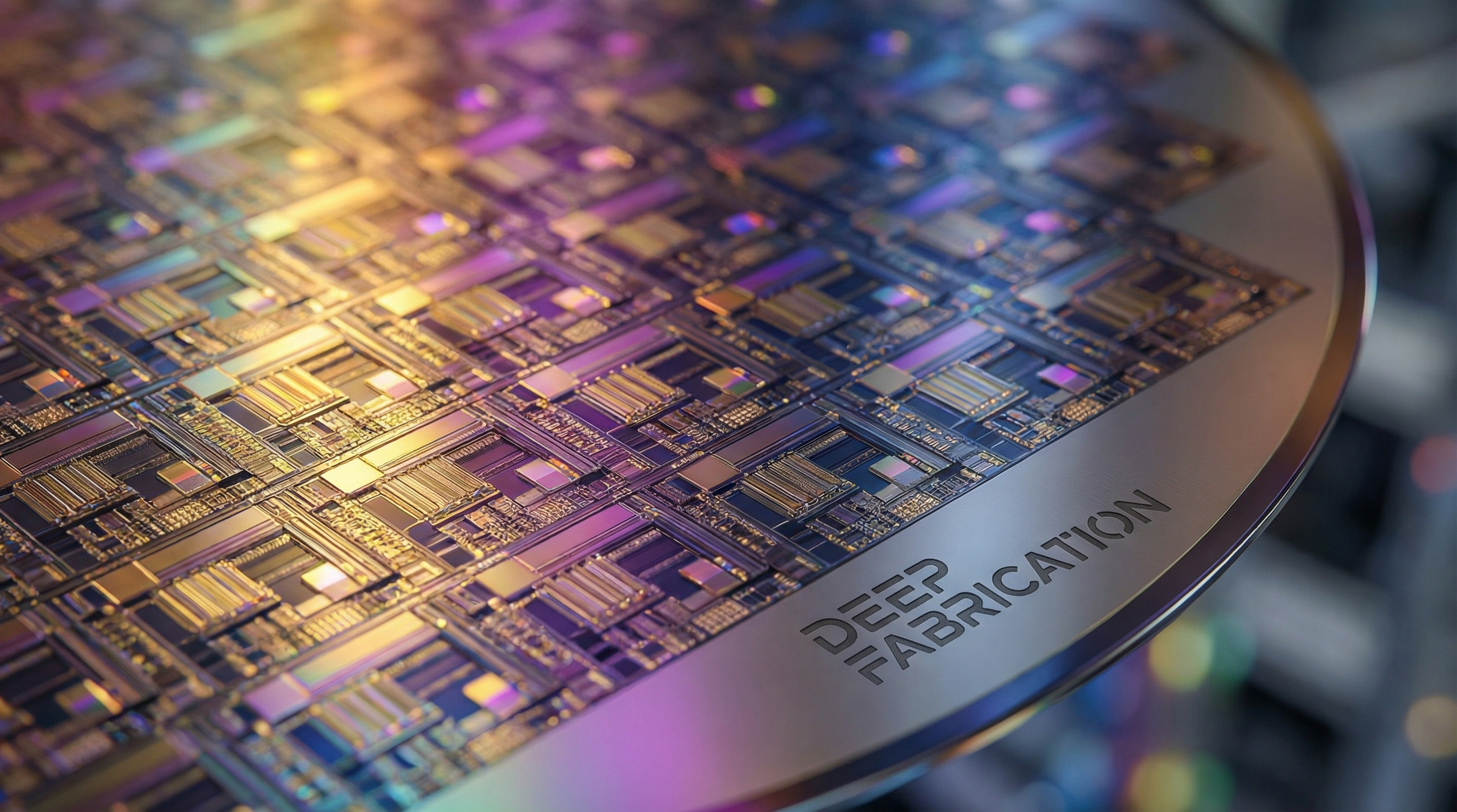
At Deep Fabrication, we’ve built deep learning models that predict fabrication defects at 1 nm, allowing engineers to optimise their recipes before fabrication begins.
Defect Prediction
Our deep learning tools predict fabrication outcomes before a single wafer is processed.
Instantaneous Results
We replace simulations that take hours with AI predictions that deliver results in milliseconds to seconds.
Closed-Loop Design
We provide a technical bridge between CAD design matrices and final fabricated patterns.
Inverse Recipe Optimisation
Our neural networks can take a desired 3D pattern and work backward to identify the exact dose, temperature, and pressure required.
Our Advantage
Real-World Data
We don't just simulate physics; we learn from reality.
Beyond Theoretical Models
Unlike EDA competitors who rely on assumptions, we train our models on real microscopy images and actual fabrication outcomes.
Unrivaled Capability
Our ability to generate, train, and verify real-world data provides an IP moat that even established EDA leaders cannot easily replicate.
Patented Technology
Our novel method provides a new technical innovation, which has been submitted for patenting.
Industrial Traction
Over 150 journal papers, 200 conference publications, and £14m in research income.
-
Supported by partnerships with established EDA companies in the semiconductor industry.
-
Secured >£1m in funding from Innovate UK, Engineering & Physical Sciences Research Council, and the Royal Society.
-
Backed by the University of Southampton, combining advanced nanofabrication capabilities with leading research in artificial intelligence.
Meet the Team
-

Dr. Yasir J. Noori
CEO & Founder
Assistant Professor at the University of Southampton with expertise in semiconductor fabrication and nanoelectronics.
-

Dr. Ben Mills
Scientific Advisor
Principal Research Fellow with expertise in AI, laser machining, and optics.
-

Ismaeil Alnaab
Scientific Advisor
Lead PhD Researcher driving the experimental deep learning prediction of nanofabrication.
Contact Us
We are now seeking pre-seed investment to scale our team and commercialise our technology to leading semiconductor foundries.
Interested in working together? Fill out some info and we will be in touch shortly.